PCB Design Overview
Article published Nov 8th 2022!
This post is intended to give you a high level overview on the key steps involved in bringing a design to fruition. Having a broader perspective on a project allows one to set appropriate timelines and ensure the work is not overloaded. Depending on the scale of the design, multiple teams may be required or one person may be adequate. The complexity of the design may also require additional tasks and respective expertise.
As an example, for a design which feature new custom components, the first task will be to create the schematic symbols and PCB footprints. Often, a library is maintained to allow easy re-use of these parts and some are even provided by vendors selling these physical components. Regardless of the method, these two ingredients (schematic part and PCB footprint) must be made available before any additional tasks can be initiated. In addition, for a design which features modern day high speed electrical interfaces, one will not only have to be diligent to follow appropriate routing guidelines with impedance controlled traces, but then a post-layout signal integrity simulation may also be necessary. This will require the appropriate IBIS models for the components of interest along with timing information to ensure there is adequate margin in the interface.

As another example, if the design is compact and modular, then multiple boards may be suitable which can be connected with a flex cable and mating connectors. Depending on the signal voltage levels and transfer speed, there may be scrutiny necessary to ensure data integrity is not jeopardized due to potential signal degradation. Connectors are notorious for creating interference in signals hence a more advanced technique has been conceived using rigid-flex circuit boards which removes this weak and susceptible link. The design will remain a single board but will feature a limited stackup in the flex region and a full layer count in the rigid region. This will drive additional constraints in the CAD tool and collaboration with the PCB vendor to ensure the stackup meets the objective. Material selection will be key to ensure the flex portion of the PCB meets bending and reliability expectations. Pursing the goal of achieving a compact design, another recent capability provided by PCB manufacturers is embedded components. This technique essentially allows smaller components to be placed in a cavity within the circuit board. This minimizes the board real estate required and brings a number of other advantages but at a significant financial expense.
Keeping in mind the points above, one will need to consider each project to be unique and assess the various parameters as a high level overview is conceived. For the particular process flow-chart shown below, this is a multi-layer board featuring several high speed digital interfaces intended for high volume manufacturing. The mass production requirement drives additional constraints for manufacturability, reliability, and testability. These are collectively referred to as DFx (DFM, DFR, and DFT). Often there are dedicated teams or individuals who specialize in these disciplines and provide feedback to the layout designer to ensure each criteria is met. As an example, for the DFM requirement the designer must adhere to strict component spacing rules to allow a high yield rate during assembly. The pick-and-place machines have a certain tolerance and that must be factored in when assigning component locations on the board. Further, rework is a legitimate concern that can be a costly and time consuming effort. Faulty components do exist and once identified on an assembled board, they must be removed and replaced. This effort is often manual and the technician needs to have enough component clearance to perform this task effectively. So for certain high risk components, a larger spacing clearance will be assigned. And on the topic of testing for faulty components, this is a prime reason for the task of ensuring the board is designed for testability. Enough test coverage needs to exist such that post-assembly, the factory can expose any abnormalities either in the PCB itself or component soldering. Ideally, all nets on a board would be able to be probed by providing a test pad or area of exposed copper but that is not often feasible or practical. Therefore, signing off on the DFT is once again a negotiation between the Test/Validation Team and Design Team.

Despite the uniqueness for each design, there are still some common tasks that exist. These include creating the schematics, generating the netlist, and importing them into the EDA tool of choice. In terms of the physical PCB, one needs to define the appropriate stackup, board dimensions, trace width and spacing, and via structure. Once routing is complete, the design is often reviewed and fabrication collateral is produced. A wide range of formats are accepted by manufacturers these days so it's really up to the designer to determine which format is selected. Regardless of the format, the vendor will further review the design, may provide some feedback, and then provide a timeline for when first boards will be ready.
Summary
As intimidating as the process may seem, it's critical one has a high level overview in mind to ensure critical steps are not missed as this is often a costly mistake both in terms of time and money. So take some to digest the scope of the project and don't hesitate to draw out a flow chart or a checklist. Having a comprehensive list of deliverables and the effort involved in producing them will set realistic goals. Identifying dependencies between the deliverables is another recommended step that should be addressed. If the design requires a mechanical enclosure or housing, certain items will need to be completed in parallel and will be iterative in nature. The PCB dimensions and component height information will need to be reviewed to ensure there is no mechanical interference or collision with the housing. For complex designs, thermal aspects will need to be assessed and appropriate measures such as vents or contact points for heat dissipation will need to be considered. Large corporations have sophisticated criteria's and processes in place to ensure successful outcomes that have been revised over the years as learnings occur. Nevertheless, we all make mistakes, but making sure we learn from our mistakes is the most important thing!
Component Placement
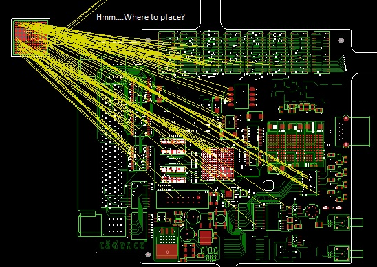
Careful placement of components is critical to a successful design
Sub-Drawing Feature
Convenient method to export sections of a design and export them into a new one.
Generate Gerbers