Generate Gerbers in Allegro PCB Editor
Article published Nov 23rd 2022!
In order to fabricate a printed circuit board, the vendor must be provided with the design collateral in a format that is traditionally known as gerbers. Although somewhat dated, this format is still widely used in the industry despite more user friendly data packages being available. The gerbers are comprised of .art files for each layer of the PCB along with the drill files. The complete dataset often also includes an IPC-D-356A file which is essentially the netlist enabling electrical testability at the fabrication house. If the design has cutouts or slots that require an additional process beyond traditional drills then a .rou file is also required. And finally, a readme text file highlighting any key information is also commonly accepted.

Artwork Films Setup
Allegro PCB Editor artwork generation requires the designer to set up the appropriate films which include the respective classes and subclasses. For example, pri.art which is the TOP layer should include the copper profile including traces, planes, component pads, and via pads. This translates to ETCH/TOP, PIN/TOP, and VIA CLASS/TOP. All copper layers will require a similar film capturing similar information as it pertains to that layer. As for the mask layers, this often includes soldermask, solderpaste, and silkscreen which need to be set up in a similar fashion and should include both component package geometry and also board geometry. The artwork control form can be accessed from the Manufacture menu toolbar and then by selecting Artwork. A similar window as shown below should be visible where the designer can set up the appropriate film definitions. The Allegro PCB Editor tool also provides a means to export and import artwork film definitions to redundant work can be avoided across different designs.

Other formats
As mentioned earlier, there are other more convenient fabrication datasets which capture design details above and beyond the traditional RS-274-X gerber package. A perfect example is the PCB stackup. Material information is not included in the gerber dataset as it's often discussed via emails or spreadsheets. A more efficient method is for communicating stackup details is thru the IPC-2581 file which serves a dual purpose as containing fabrication data as well. Another example is the assembly data which is needed during component soldering at the pick and place machine. The X-Y coordinates for each component need to be provided to allow correct population of parts on the PCB. Once again, the advanced IPC-2581 file is capable to include this comprehensive information such that multiple seperate gerber datasets are not necessary.

Z-Copy
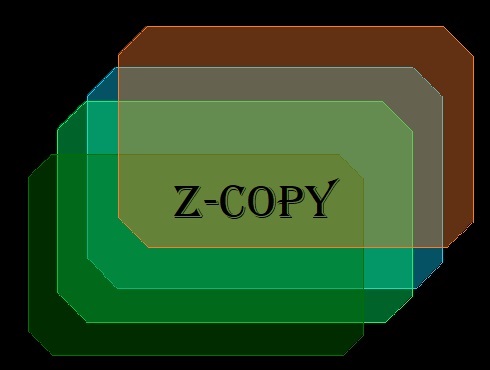
Best kept secret in Allegro PCB Editor for copying shapes across layers
Thermal Relief
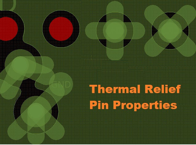
Pour large regions of copper in your design using shapes
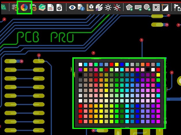
Color Settings