Constraint Manager in Allegro PCB Editor
Article published Nov 30th 2022!
Prior to beginning the task of component placement and trace routing, it is wise to set up appropriate design constraints. These are parameters defining things such as the board outline, component spacing constraints, copper feature constraints, and any other specification that we would like the EDA tool to track. Defining these constraints up front and early allows the designer to take advantage of the live Design Rule Check (DRC) feature which flags a violation as soon as it happens rather than iterative post-processing checks. Although constraints are highly recommended, one should also be mindful of the possibility of over-constraining the design. This could trigger an abundance of irrelavant DRC's which can be overwhelming at a time where focused clean-up and polishing is needed prior to releasing a board for tape-out. Standard process is to either resolve the DRC by fixing the violation or waiving the DRC with an explanatory note.
Allegro PCB Editor provides a spreadsheet like format for capturing design constraints in the tool known as the Constraint Manager. This tool can be opened from the Setup Menubar and highlighting Constraints->Constraint Manager.
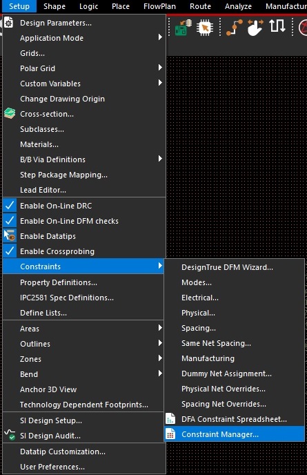
Another faster method is to use the shortcut icon from the toolbar which looks like a spreadsheet.

A seperate window should open with several sections visible in the left side-bar. At a minimum, the designer should specify the Physical, Spacing, and Manufacturing constraint sets. Depending on the complexity of the design, appropriate constraints should be enabled to optimize the DRC feature.
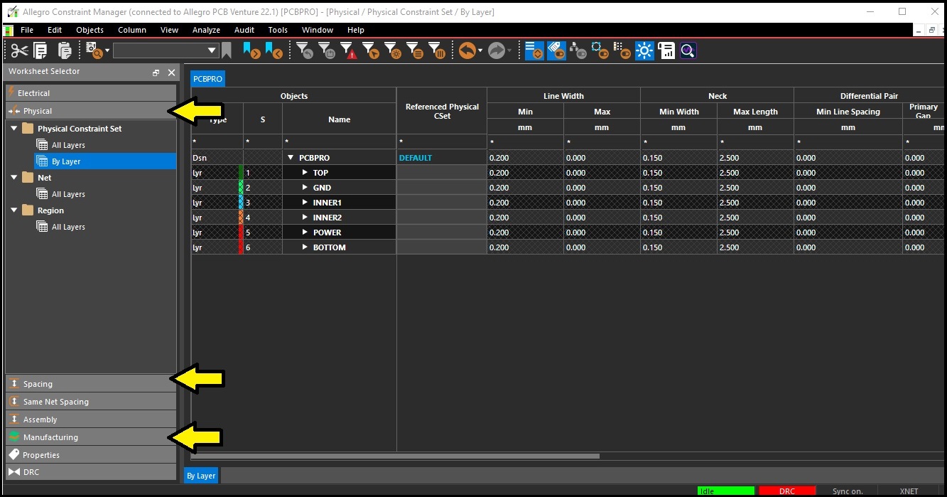
If differential traces are used, then respective properties such as trace spacing and neck length, etc should be specified and if blind/buried vias are used then via staggering distance may be a useful constraint. It may not be evident which constraints are necessary for beginners and this is where it's encouraged for the user to take their time and explore the comprehensive features Allegro provides.
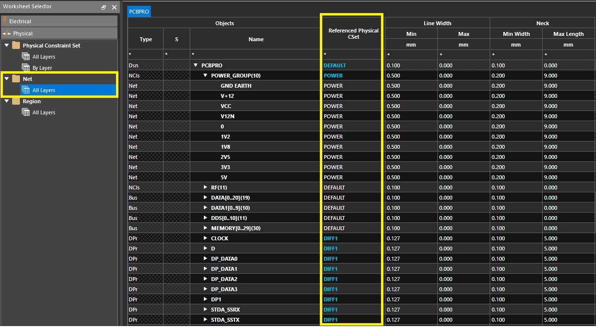
Physical Constraints
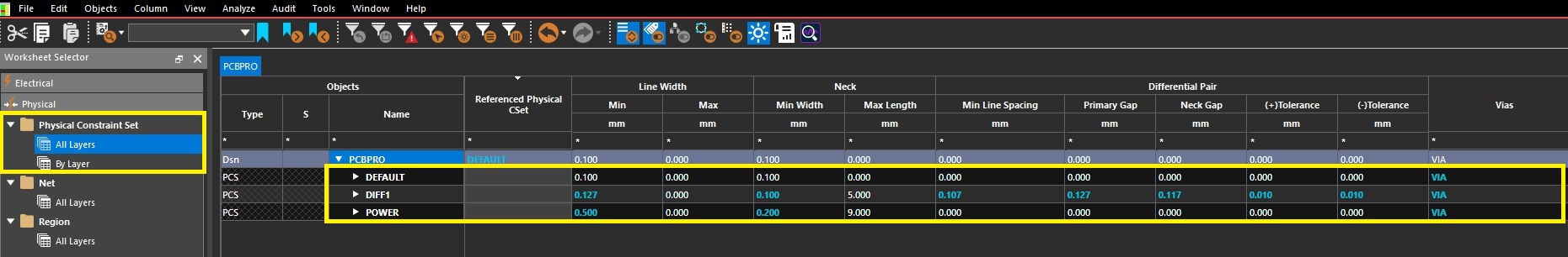
Trace width is a parameter that needs to be defined before any routing can begin. During stackup discussion, the PCB vendor may provide a recommended value and if the designer is in agreement then the constraint manager is the location to feed that input. Typical values in the industry for single-ended traces are anywhere between 0.06mm to 0.1mm for which dielectric height can be set to meet a 50ohm impedance. For traces carrying power signals, the width is desired to be as thick as possible and so a minimum width value should be specified.
A recommended approach is to create "Referenced Csets" which is essentially a group of nets that inherit the same constraints. This effectively optimizes the task of setting up constraints in the tool. As an example for a simple design, a Cset could be created for the power nets, single-ended signal nets, and differential nets. Once values are defined within these Csets, then the respective signals can be mapped accordingly.
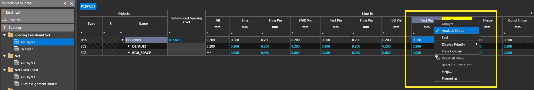
Spacing Constraints
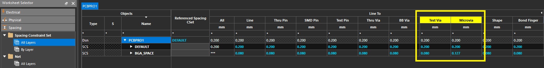
Allegro PCB Editor offers many spacing constraints to consider, some of which may not be applicable to a given design. In such cases, the user has the option to disable the respective checks which are not relevant. This can be done in one of two ways. The specific DRC can be turned off by right clicking on the column header of the constraint in the spreadsheet and selecting Analysis Modes. The column header will change to a yellow background indicating the DRC has been disabled.
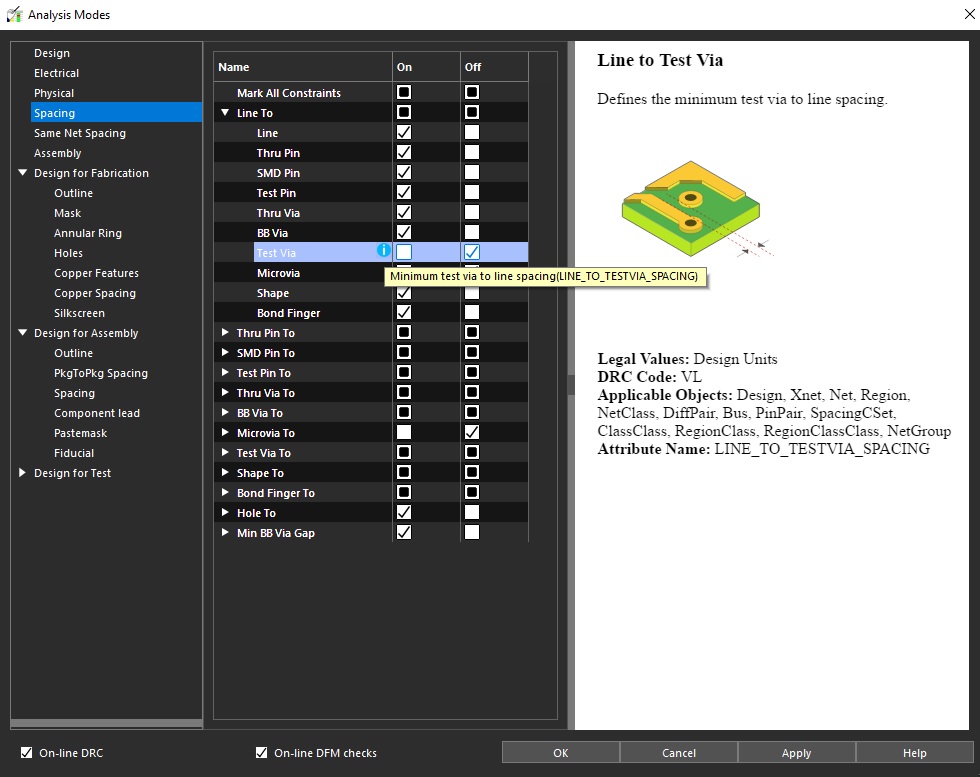
The other method is to select Analyse from the Menu taskbar and click Analysis Modes from the drop-down. This will open a new window with constraint categories listed in the left side-bar. Upon selecting the category of interest, the main section in the window will update with the individual DRCs and checkmarks will indicate active/inactive items. To learn more about a specific constraint, hovering over the Information icon will update the right side-bar with additional details. It's worth mentioning, if not already obvious, this is an excellent way to explore and learn the extent of constraint management options Allegro PCB Editor offers.
Manufacturing Constraints
The Manufacturing section captures constraints pertaining to the board fabrication and board assembly. While both are equally important, the fabrication constraints are typically already captured as part of the Physical and Spacing definitions. Defining them in the Manufacturing section could be a redundant effort but could also serve to be useful depending on the design. The focus should rather be on the Design For Assembly (DFA) portion which is critical for ensuring component placement spacing.
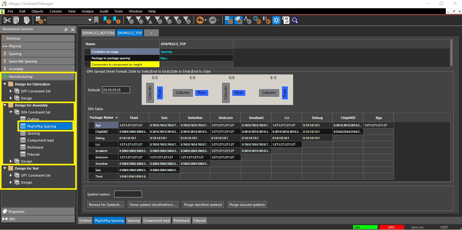
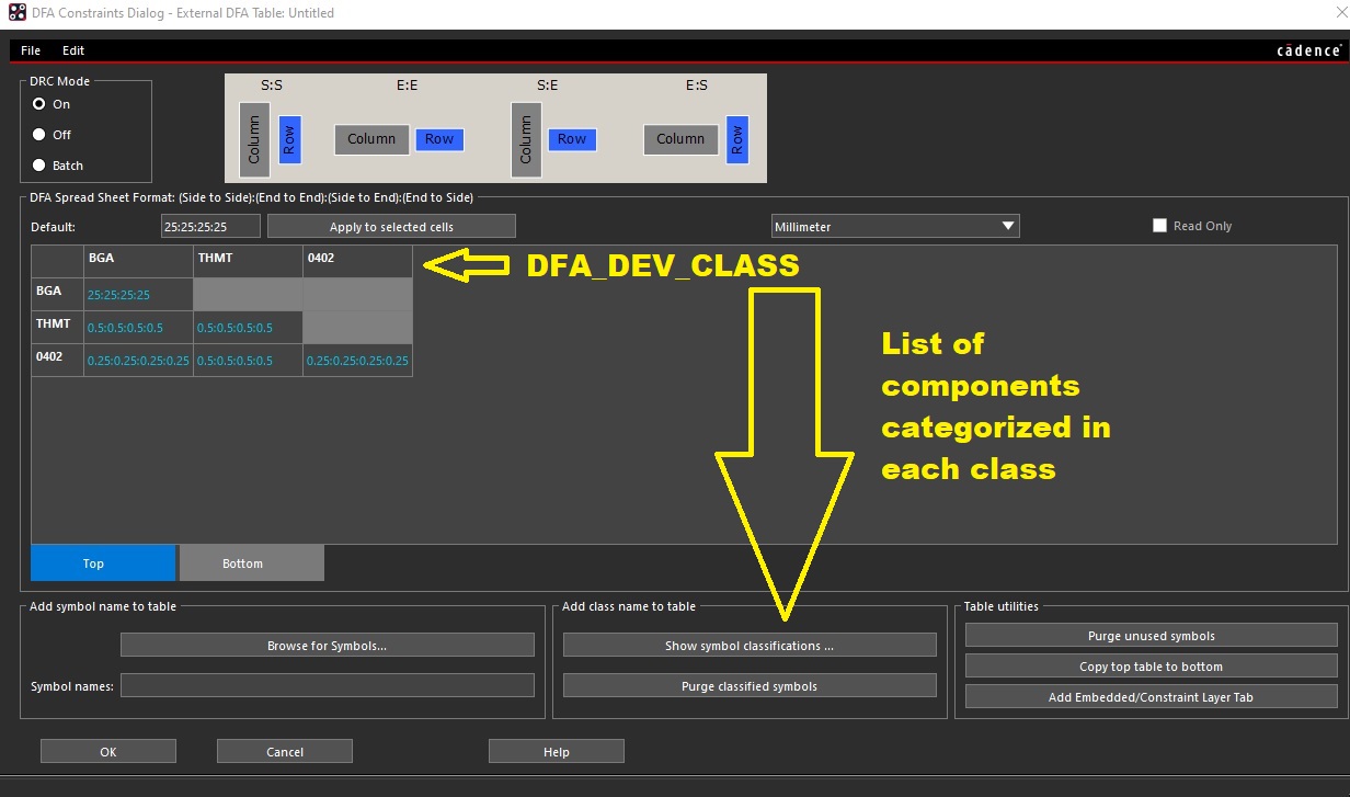
The DFA table can be generated within the Constraint Manager or produced thru a separate tool known as the DFA Spreadsheet Editor. Component spacing constraints are set based on the DFA_DEV_CLASS which is a category assigned to each component in the library or design. For example, a DFA_DEV_CLASS may be created to organize all 0402 components. Another DFA_DEV_CLASS would capture BGA parts, and another for thru-hole parts. The spacing requirements to ensure high-yield assembly should be provided by the facility tasked with soldering components to the PCB. They may have smaller clearance requirements between 0402 components to BGA components and larger clearance requirements for 0402 components to thru-hole components. The spreadsheet table captures these spacing requirements for all orientations across all DFA_DEV_CLASS categories. During the component placement task, the on-line DRC will provide real-time feedback if components are being placed in violation of spacing constraints as defined in the DFA table. To ensure this effort is not duplicated for each design, Allegro PCB Editor allows the user to export and import this DFA table making this a very convenient and powerful feature.
Re-using Constraint Sets
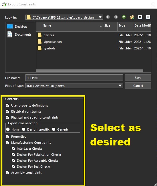
As mentioned earlier, leveraging constraints from existing designs is a great mechanism to gain confidence for new projects. Not only does this accelerate the layout phase of the design but also ensures any critical constraints are not missed when beginning a new design that may be in fact be similar in nature to a previous one. Upon exporting the constraints, the user has the option to select the level of details that are desired and check the boxes accordingly. At the time of importing the constraints file in the new design, an informative report is generated highlighting the updates and differences.
Summary
This post only scratched the surface on the potential for the Allegro Constraints Manager. An abundance of parameters exist which can be defined to set a rigorous criteria for designing a printed circuit board. The Physical, Spacing, and Manufacturing Constraints are the bare minimum that should be considered. Rather, users are encouraged to explore the full suite of offerings and create a template that can be leveraged across their design portfolio. The intuitive export and import feature is note-worthy and highly recommended. Effort exerted in setting up thoughtful constraints in a master design are not wasted and can be utilized across numerous projects. Aside from showcasing how to set up specific design constraints, the other motivation behind this article is to stress the importance of defining the constraints early in the design cycle. As the design progresses, it's best practise to clean up violations as they occur rather than letting them accummulate. A final DRC clean-up effort can be triggered as the design approaches completion and is queued for a tapeout review. A report is often generated highlighting any existing DRC's and a comment is captured to indicate the reason for allowing the waiver. Diligent documentation in this regard gives confidence that fabrication and assembly will be successful leading to a functional design.
Z-Copy
Best kept secret in Allegro PCB Editor for copying shapes across layers
Thermal Relief

Pour large regions of copper in your design using shapes
Color Settings