Z-Copy feature in Allegro PCB Editor
Article published Dec 5th 2022!
Creating and modifying power and ground planes is a common task when performing layout activities. An effective way to copy shapes to different layers in a single step can be executed by utilizing the Z-Copy function. This handy feature can be accessed from the Edit Menu and although this article highlights the capabilites of Z-copy for shapes, it works just as effectively for traces as well.

When Z-Copy is selected, the designer should review the Find Filter to confirm which object(s) is selected and if that aligns with their intention. Once confirmed and selected accordingly, switch to the Option tab and make further selections. The layer on which the copied contents are to be pasted can be specified by changing the Class and Subclass dropdowns. If a shape is being copied, then additional options can be considered whether the shape should be created as a dynamic fill and if any net properties or voids should be propogated. Additional sizing options can also be modified to either contract or expand the shape by a specified offset value. Once all parameters are confirmed, the task is as simple as finding the shape of interest on the canvas and clicking it. If multiple objects are being copied simultaneously, then a box can be drawn around them. The new layer (Class/Subclass) will automatically become visible and the Visibility pane can be used to hide the current layer view to confirm the copied content is as expected.

It's worth mentioning that shapes and lines are not restricted to only ETCH layers. These objects can exist throughout the design and are commonly found on FAB sheets as well. FAB sheets are typically included as part of the gerber package which provide the PCB vendor additional information pertaining to the design. There can be notes specifying the soldermask colour, surface finish, or even highlighting certain regions of the design and confirming manufacturing requests. For example, PCB vendors usually place their own markings on the PCB they produce and sometimes they may put these markings in an undesireable location. It may be undesirable due to cosmetic reasons or could also potentially impact design functionality. In either case, the designer can in fact specify locations for vendor PCB markings. The Z-copy is a feature that can be used to copy the design outline, component outlines, and key copper features as desired to the FAB sheet and then mark them up accordingly.

Routing Traces
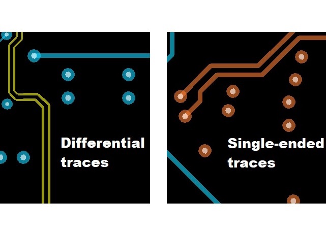
Diligent routing is critical to ensure a successful design
Shapes
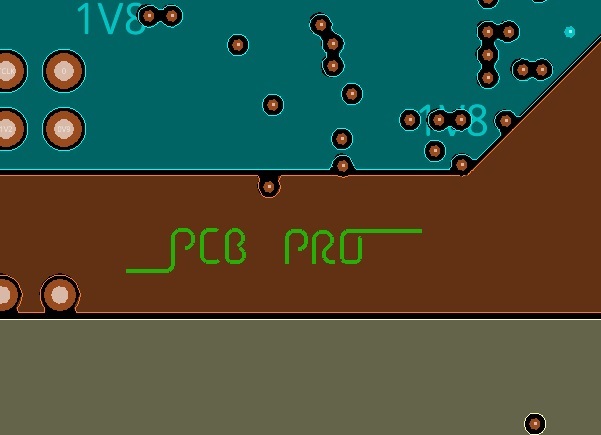
Pour large regions of copper in your design using shapes
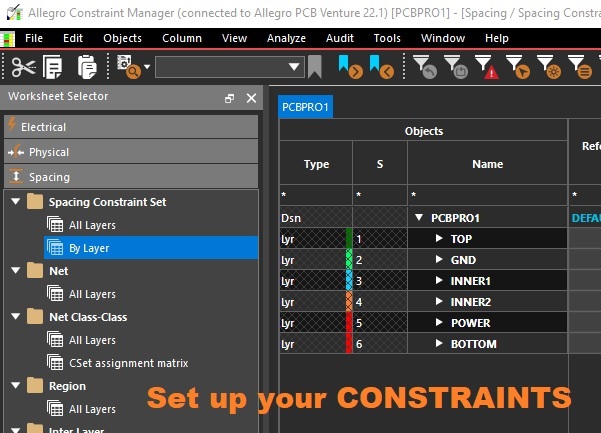
Constraint Manager