Routing Traces in Allegro PCB Editor
Article published Nov 25th 2022!
Electrical connections on a circuit board require a conductive material which is often copper. The EDA tool is used to draw these traces and the manufacturing facility builds the boards accordingly. Drawing these traces in Cadence Allegro PCB Editor is relatively easy and can be initiated once the design netlist has been imported. The netlist captures the logical connections between components whereas the board routing defines how these connections are made physically on the printed circuit. The task of making these physical connections often becomes more complicated as the number of components increase in a design. The pin count of each component is also another contributing factor. In order to physically makes these connections, often enough a multi-layer board is required. Vias are typically used to traverse these layers and depending on the layer count and complexity, uvias (microvias) are utilized to allow connections to occur between selective layers. Setting up the EDA tool to allow the user to begin routing traces requires a number of steps.
Define trace characteristics
Typically at the time of stackup creation, one needs to understand whether the design will feature any high speed digital signals. If so, then most likely the design will require impedance controlled trace definitions. An oversimplified definition of Impedance controlled means the fabrication facility will ensure the copper traces, layer lamination, and material composition will all be manufactured within a tight tolerance. For the EDA user, they only need to worry about setting up their design based on the trace dimensions provided to them by the PCB vendor. For single-ended traces, a trace width will be give and most likely the most immediate layers are the reference planes. For differential traces, both a trace width and trace spacing will be provided. The reference plane in this case can either be a immediate layer(s) or skip a layer. This gives the flexibility in meeting impedance requirements and ensuring trace width and spacing dimensions are actually manufacturable.


Set up Via definition
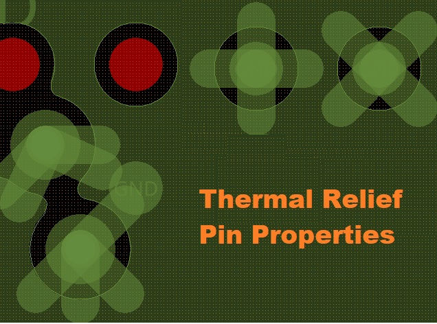
Setting up vias to use in your design requires a few additional steps but also brings forward some customatization capbilites. The Padstack editor is used for creating via definitions. The via pad shape is firstmost attribute to define and most commonly it's a circular shape. The drill size is determined and for more complex vias which require backdrilling, then a secondary drill is also required. The default thermal relief connection profile can be defined along with any specific mask openings and pluggings. Once all these attributes are set, the via padstack should be saved and then referenced in the project design.

A key step which often gets missed and raises chaos among new Cadence users, is the task of updating the padstack path variable to the appropriate location. This can be set by Selecting "Setup" from the Menu taskbar, and clicking the "User Preferences". In the window that pops up, select "Paths" in the left pane followed by "Library". In the right pane, you will see the variable "padpath" for which you can click the horizontal ellipsis (three dots) and add the directory which has the via padstack that was recently created.

Route signals
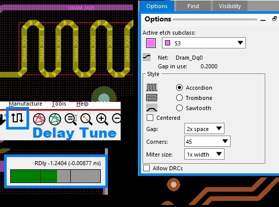
With the design constraints set up correctly, one can finally begin the exciting task of routing. Having a high level strategy is critical to ensuring the design can be fully routed within the layer and via definitions. The RatsNest is a great indicator for showing the remaining connections that need to be traced. Once the Route feature is activated, the Oject Finder can be used to select "Pins" and the Options window can be used to customize the routing characteristics. Options such as trace bending characterists (45,90,arc), and object interference can be set accordingly as based on personal preference. To traverse layers, one can Right-Click and select "Add Via" or simply perform a double click on the canvas at the location they want to drop the via. The trace will continue at the appropriate layer as selected in the Options window.

Summary
Routing traces can often be misunderstood to be a trivial task but if attention to this task is neglected, the consequences can be quite fatal. Especially in the realm of high speed digital designs, certain principles must be followed to ensure the signals can propogate as expected. If traces carrying high frequency signals are routed over voids in their reference planes then the current return path is no longer taking the path of least impedance and will be forced to take other paths which will not only degrade signal quality but also create additional electromagnetic interference issues. Debugging these sorts of issues is both time-consuming and expensive as often enough a board spin will be necessary. Post-layout simulation has become a common task to ensure such mistakes are caught prior to designs taping out.
Watch Demo! - Like & Subscribe!
Z-Copy
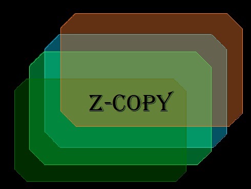
Best kept secret in Allegro PCB Editor for copying shapes across layers
Thermal Relief
Pour large regions of copper in your design using shapes
Trace Length Matching