Setting up Thermal Relief in Allegro PCB Editor
Article published Dec 10th 2022!
Component soldering is a science which requires precise control over the temperature to ensure adequate melting and solidifying of the solder to bridge and hold the connection between the component pin and the PCB pad. To assist in facilitating this task, the circuit board can be designed such that the copper pad heat distribution profile is controlled. It's common knowledge that metal conducts heat well and the larger the surface area, the easier the heat is dispersed. But that also means it takes longer to heat that specific area if it's well connected to surrounding metal.
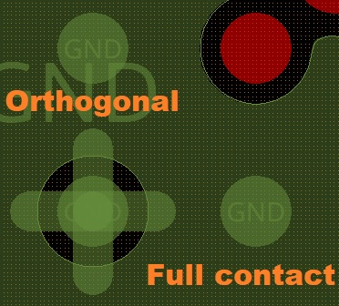
Essentially, the rate of change in temperature at a specific pad will vary depending on how that pad is connected to surrounding copper. Thermal relief definitions for these pads is what determines how these pads will heat and cool when undergoing the assembly process. A "full contact" pad will heat slower compared to an "orthogonal contact" pad.
So imagine if a 2 pin component has one pin which is to be soldered to a full contact pad and the other pin is to be soldered to an orthogonal contact pad. The difference in the thermal characteristics may cause one side to heat faster than the other side causing the solder to melt at an uneven pace. The side on which the solder has melted sooner will create tension on the component and potentially shift the components location away from it's ideal spot. If the shift is significant enough, then the other pin may not even be able to form a connection with the copper pad resulting in an open circuit. Unfortunately, this is a common enough occurence with certain components (0201 dimension or smaller) where pad thermal relief contacts are not given proper attention. These small 2-pin components end up soldered in a vertical configuration due to a formed solder connection only on one side mimicing a tombstone at a cemetery (hence the phenomenon described as "tombstoning".
Pin Properties
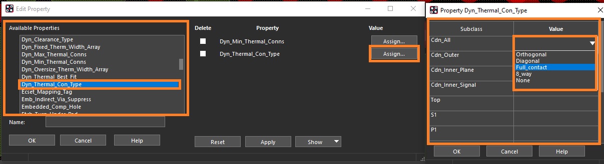
An easy method to modify the thermal relief properties of an individual pin or group of them is to select the Pins in the object filter and highlight them. Once highlighted, right-click and select Property edit. A dialog will open and scroll down to select Dyn_Thermal_Con_Type. The property will be visible on the right side from which the Assign button will open another window. The user now has the option to specify the thermal relief configuration on a per layer basis. This would be more so applicable to vias where they may connect to nets on internal layers as well. For a component pin, either top or bottom should be sufficient but sometimes for convenience Cdn_All is selected. The drop-down allows selection of the following options: Orthogonal, Diagonal, Full Contact, 8_way, or None. Additional properties can allow be modified for precise control on the thermal relief connection profile. The spoke thickness and number of contacts are examples of properties that can be adjusted. Once all options as desired are specified, clicking the Ok or Apply will do an immediate update to the selected objects.
Global properties
It is always recommended to have global properties set for default thermal relief connections. This minimizes the additional task of checking each pin that may be affected. The Global Dynamic Properties can be set thru the Shape Menu and selecting Global Dynamic Params... In the window that opens, navigate to the Thermal relief connects tab and you'll be presented with numerous customization options. The contact style can be globally set for Thru pins, Smd pins, and Vias. In addition, for any contact types which feature spoke connections, the number of contact points along with the spoke thickness can also be defined.
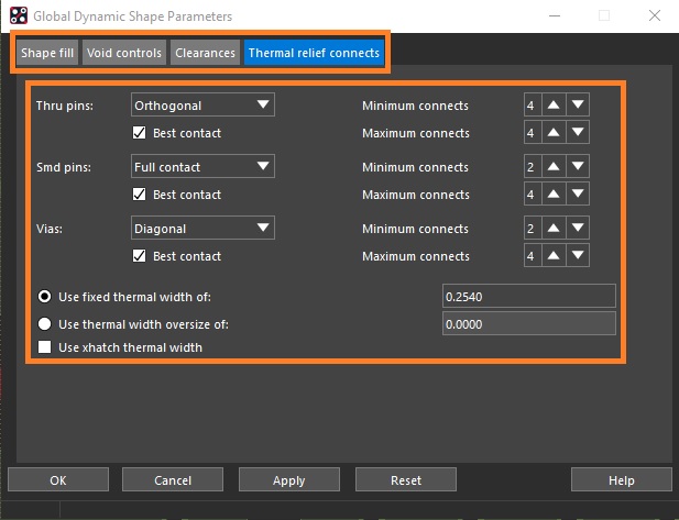
It's important to ensure that the Best Contact checkbox is selected so the tool has permission to adjust the spoke connections to allow for contact points to exist in conditions where the minimum criteria does not meet. Otherwise, if a pin is not able to make a connection due to the minimum contacts specified, then that pin will remain unconnected leading to an open circuit. As an example, the Via contact is set to Diagonal style with minimum connection points to 4. If the Best contact feature is not enabled, then one case yields no connections at all.

Summary
We've explored two methods to set thermal relief properties to pins and vias. They can be set at a global level which impacts all objects or modified as needed for particular objects. In terms of precedence, the individual modification takes priority over the global setting as one would expect. To confirm if a pin property has been modified to deviate from the global setting, you can right-click the pin and select Show Elements. Parameters which have been manally defined for that object will be clearly visible for review. They can be reverted by deleting that pin property in a similar fashion to how it was initially assigned or another approach could be to unplace and place that symbol. The symbol could also be refreshed along with it's padstacks to bring back the default characteristics and apply the global thermal relief settings.

Routing Traces
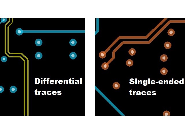
Diligent routing is critical to ensure a successful design
Shapes
Pour large regions of copper in your design using shapes
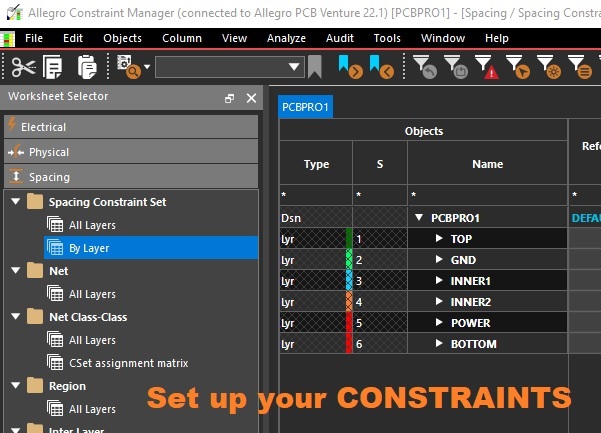
Constraint Manager