Exploring Shapes in Allegro PCB Editor
Article published Nov 28th 2022!
Assigning large areas of copper on the board is often accomplished by using shapes in the EDA tool. These regions are typically assigned to power and ground nets which are critical for current delivery. A large surface area to facilitate this energy transfer is desireable as it minimizes resistive losses. On a multi-layer circuit board design, several layers are dedicated as "Plane" layers which serve two key roles.
1. Power distribution to components
2. Reference plane for high speed impedance controlled traces
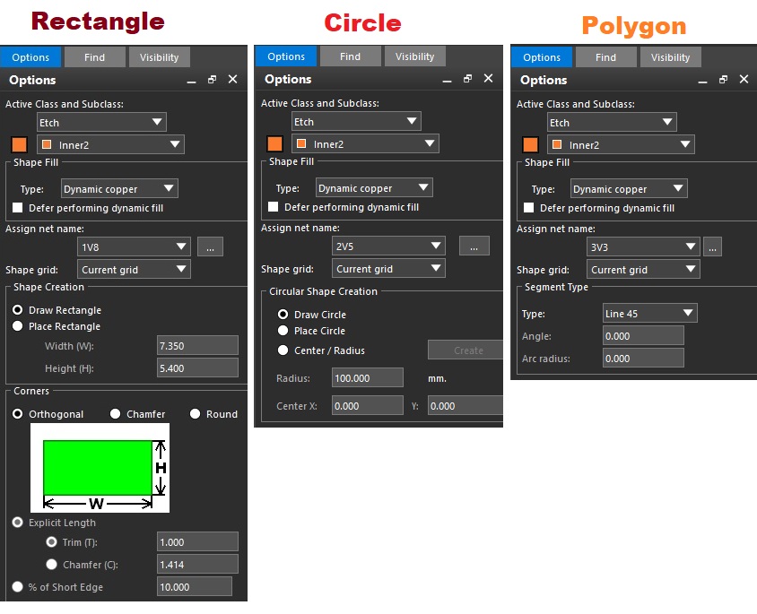
Both of these requirements can be fulfilled by careful placement of copper shapes on selective layers. In Allegro PCB Editor, the designer has the option to place rectangular or circular shapes based on pre-defined dimension or they can draw them to a custom size. In addition, the designer also has the flexibility to create polygon shapes by drawing out their desired region. Upon completion of the shape on the canvas, the net can be assigned from the Options window on the right sidebar.
Shape priority
It is not uncommon to have multiple shapes on a given layer and to ensure maximum coverage exists, the shape outlines could be overlapping. If such a situation arises, then Allegro PCB Editor utilizes the "Shape to Shape" spacing value as defined in the Constraints Manager. In terms of which shape takes priority, the designer can select an individual shape and right-click to either lower or raise it's priority level. Raising the priority will bring this shape to the top and it's outline will override any overlapping areas with other shapes. The opposite will occur when a shape is selected and it's priority is lowered.
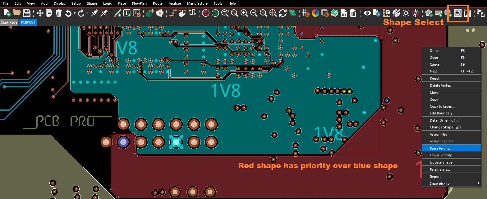
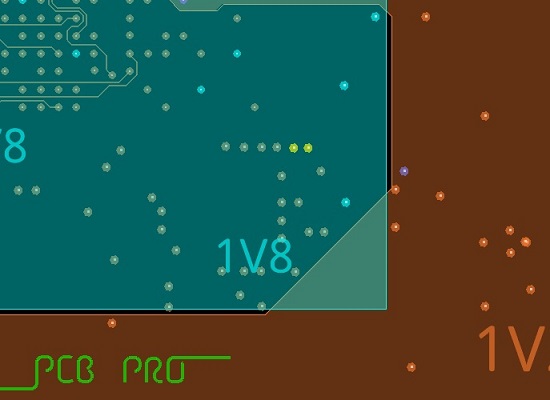
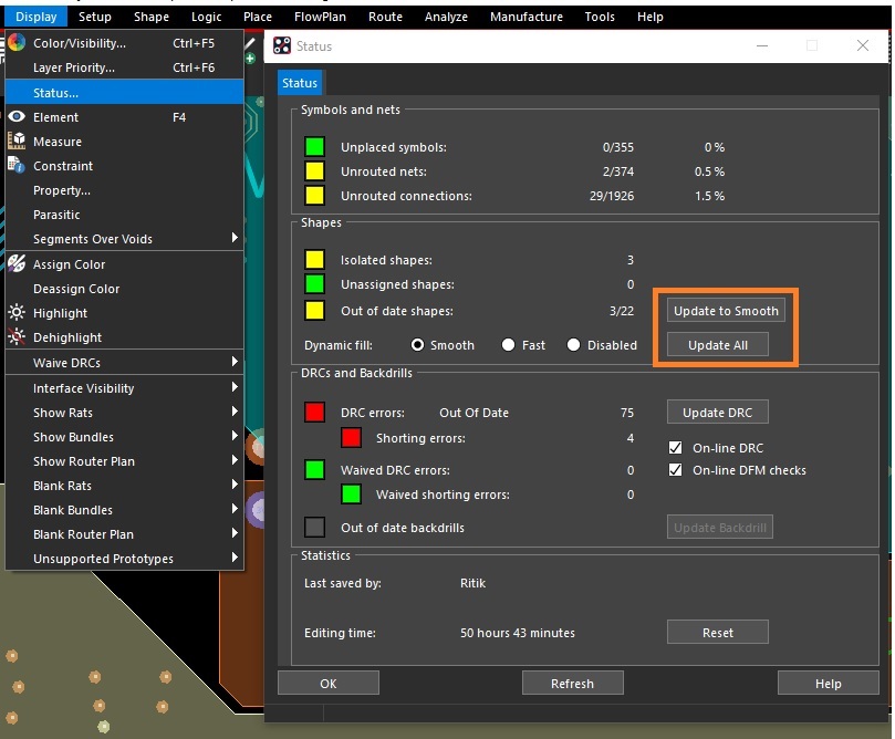
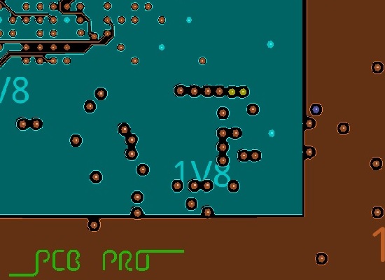
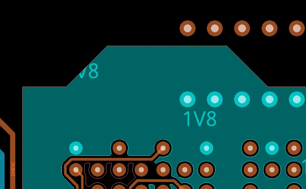
One key step that needs to be done after making any shape priority changes is to update them so their dynamic characteristic can be re-enabled. As seen with the example below, the blue shape priority has been raised so it's corner which was previously underneath the red shape is now on top. But other spacing constraints associated with this shape have also been temporarily lost as seen with the trace and via objects which are no longer maintaining their clearances with this 1V8 power plane. A "Shape Update" is required which can be initiated thru the Display menu dropdown and selecting Status. In the window that pops up, make sure the radio button next to Smooth is selected and click either Update to Smooth or Update All. The shapes should all refresh and the latest change made to the priority will become visible.
Edit Shapes
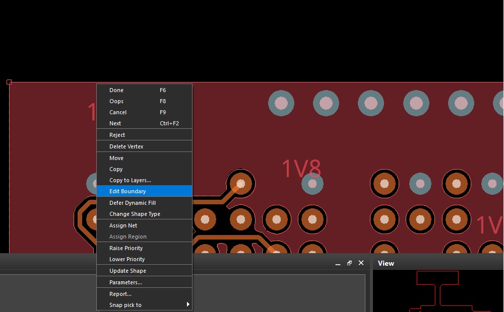
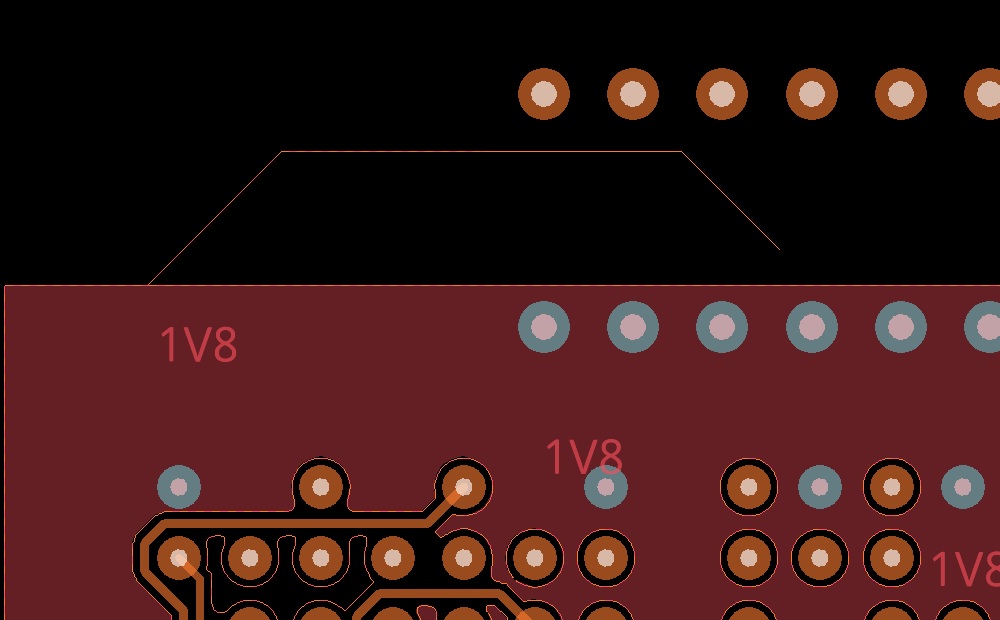
There are many occasions which require one to go back and make modications to a shape. It's not quite practical to re-draw the shape and fortunately within Allegro PCB, the designer has the option to make selective edits. Upon selecting the shape, the outline becomes activated and can be moved as desired. A small square will also be visible at each vertex that can be moved to a new location at which point the shape will update accordingly. A more advanced technique is to edit the boundary and redraw only a portion as needed. This can be done by right-clicking on the shape once it's been selected and clicking "Edit Boundary". A similar operation as creating a polygon shape will be triggered giving the designer the freedom to draw the extension of the shape as they see fit. To complete the shape, one can bring the final connection back to a point on the existing shape boundary or right-click and take advantage of the "Complete shape" function which automates the final link.
Shape Voids
Manual cutouts in copper shapes are implemented by designers for a number of reasons. Either they would be to increase clearance from certain sensitive vias or traces on the same layer or to maintain impedance requirements for differential traces which reference a plane deeper into the stackup (skipping the immediate layer above/below). Regardless of the reason for the shape void, they can be created very easily in Allegro PCB Editor. Select Shape from the menu taskbar, expand "Manual Void/Cavity" and pick the desired option. If a circular void is selected, then click the shape of interest, draw the circle at the desired location, and right-click -> Done. That's it!
Although very simply to create a manual void within a shape, the designer needs to be aware that if the shape is moved or re-drawn, the void will behave accordingly. It is recommended the shape which has critical voids be "Fixed" such that accidental modifications cannot be made. This can be done by selecting the shape and right-clicking to pick the Fix option. Similarly, when the fix property needs to be removed, the shape can be selected and "Unfixed". A more thorough method of implementing shape voids at specific locations is using route keepout regions. To be precise, these are not exactly voids in a particular shape but rather another 'shape object' which ensures no copper feature can exist within that boundary.
Summary
Knowing how to create and edit shapes in Allegro PCB Editor is a critical task that will most likely will be required in every design. At a minimum there will be a power delivery plane and a ground plane. The size of the board, along with the complexitiy of the design will drive the number of power rails and their layout. In high power designs which carry large amounts of current, the designer can also specify copper thickness for certain layers to minimze any resistive losses. Careful upfront consideration of crosstalk, EMI, and return current flow thru power planes will save time, money, and headaches during validation. So while this article introduces the reader on how to create shapes within the ECAD tool, it only scratches the surface on power delivery design principles.
Watch Demo! - Like & Subscribe!
Z-Copy
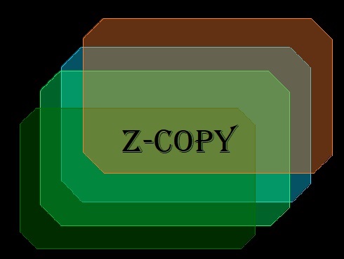
Best kept secret in Allegro PCB Editor for copying shapes across layers
Silkscreen Markings
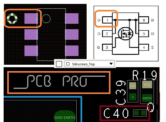
Learn how to add key silkscreen markings to your design in Allegro PCB Editor.
Color Settings