Adding Silkscreen Markings
Article published August 26th 2023!
Silkscreen is typically an optional layer within PCB designs but one that if utilized, it can offer many advantages. The visual aids on a printed circuit board (PCB) can provide information about components, reference designators, polarity, orientation, and other important annotations. These markings are added to the top and/or bottom copper layers of the PCB to aid in assembly, testing, and troubleshooting. In the example image shown below, we can see the orange box highlighting the company logo, blue box showing the pin 1 circular marking for the respective component, and various other RefDes with one explictly in the maroon box.

Component Reference Designator Markings
One of the most common markings on the silkscreen layer is to identify the reference designator (RefDes) of the various components. Adding this information to the silkscreen layer on a printed circuit board serves several important purposes:
Assembly and Manufacturing: During the PCB assembly process, electronic components need to be placed on the correct locations as specified in the bill of materials (BOM). RefDes markings on the silkscreen layer provide clear visual guidance to assembly technicians, ensuring that each component is placed accurately.
Troubleshooting and Debugging: In case of PCB testing, troubleshooting, or debugging, having reference designators on the silkscreen layer makes it much easier to identify and locate specific components. This expedites the process of identifying faulty components or verifying connections.
Documentation: Silkscreen markings contribute to the overall documentation of the PCB design. They create a visual link between the physical components on the board and the schematic design data. This is especially important if the PCB design will be handed over to another engineer or manufacturer for future revisions.
User Assistance: For end users who might need to interact with the PCB, having reference designators on the silkscreen layer can help them identify components when following instructions in a user manual or during maintenance.
Although there isn't a standardized specification on the RefDes marking or numbering convention, the general expectation is that it will be consistent within a particular design. Having said that, one common convention as follows. Components are assigned designators based on a combination of a letter representing the component type (e.g., R for resistor, C for capacitor, U for integrated circuit), followed by a numeric sequence. For example, R1 represents the first resistor, C2 represents the second capacitor, and so on. The information should match the RefDes assigned in the schematics and is typically carried within the netlist. If the generic footprint symbol has a RefDes layer present, then the numeric value will automatically update. To make this content visible in the Allegro PCB tool, navigate to the RefDes class in the Options pane and select either the Silkscreen_Top or Silkscreen_Bottom subclass depending on the placement location. Enabling the layer should then make this information visible in the surrounding region of the component.


Component Pin and Polarity Markings
It is critical the correct orientation of symmetrical parts and polarized parts be identified on the PCB to ensure proper assembly at the manufacturing lines. An incorrectly soldered component will not only deem the circuit to behave in an unexpected fashion but debug will also be a nightmare. Therefore, take caution during the design process to ensure proper markings are visible and legible on the PCB.
Pin Markings: Each pin of a component, such as an integrated circuit (IC), resistor, capacitor, or transistor, is numbered or labeled to indicate its function or connection. The numbering or labeling is usually done with numbers or letters, and sometimes symbols or abbreviations are used. Connectors are often another component which have pin markings visible on the PCB. It is not critical to have all pins labelled but rather enough to ensure correct assembly. Typically, the Pin 1 indication is sufficient as shown in the example below as the other pins can then be referenced from the schematics or component datasheet.

Polarity Markings: When a component has a positive terminal and negative terminal, then it is crucial it be populated in the correct direction otherwise disastrous events can occur. Think exploding electrolytic capacitors. To prevent such mistakes, the positive terminal node is often indicated in the silkscreen layer as shown in the example below. Diodes are another two terminal device which often require polarity markings to indicate correct orientation. Misplaced diodes may not suffer the same consequences as electrolytic capacitors but the circuit will definitely fail to function as expected leading to a different kind of confusion explosion!

Adding Text or Shapes to Silkscreen
Generating manual text or shapes to the silkscreen layer is quite common and fairly easy to do in Allegro PCB Editor. Begin by selecting the "Add Text" feature and indicate where you want to place the content on the PCB design canvas. Before you begin typing, make sure to select the appropriate Class and Subclass such that it will be printed on the Silkscreen layer. Allegro PCB Editor has several default Classes which have a silkscreen Subclass layer.

The RefDes class is specifically utilized for linked component markings so any edits within that class/subclass will need to be tied to a particular part. For example, if the component symbol is moved to a different location, the linked RefDes silkscreen marking will also shift accordingly. Understanding this behaviour, one needs to consider what is the intent of the additional text that is being created. If there is no dependency or linkage of the new text that is being added, then it may be more appropriate to add it to the Silkscreen subclass under the general Board Geometry Class.
Setting up the Silkscreen film for manufacturing
Adding the various refdes information, pin marking, and custom text or shapes to the silkscreen layers is great but the artwork films need to be set up correctly as well. This will ensure the PCB vendor will get these .art files as part of the gerber dataset package. A new film titled to indicate silkscreen top and silkscreen bottom should be created and the respective Class/Subclass layers should be added. As we noticed previously, Allegro PCB Editor provides numerous Silkscreen subclasses by default but not all necessarily need to be added to the artwork film. Only select the ones which contain content of interest that need to be printed on the silkscreen layer on your PCB design!

Summary
Silkscreen is typically seen as an optional or nice-to-have feature in PCB designs but in fact can prove to be an essential addition based on the complexity of the design. It is used to denote component refdes and orientation information along with any other information that would be useful visible immediately on the PCB. A common trap is to over populate content on this layer which tends to diminish it's value given how cluttered and chaotic the resulting design ends up being. Neatly placed text, markings, and logos will ensure the end user actually appreciates this information and also justifies the potential additional cost. This article only covers the basic elements pertaining to utilizing the silkscreen layer, stay tuned for advanced features within Allegro PCB Editor which not only enable silkscreen design rule checks, but also a very efficient feature known as Label Tune which semi-automates the silkscreen refdes text placement!
Component Placement
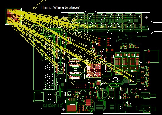
Careful placement of components is critical to a successful design
Schematic Capture
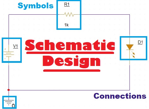
Creating schematic symbols, drawing the circuit, and generating the netlist
Generate Gerbers