Cadence Schematics Capture tool
Article published Jan 13th 2023!
The schematics of a design is essentially the starting point and the backbone of the project. This step needs to be executed with great attention as any error introduced here will propagate thru and trigger significant effort to correct later. In regards to the key tasks which are categorized as part of the schematic domain, they include the following:
Creating the schematic symbol
For custom parts this step will be required and need to be performed carefully by referencing the respective datasheet. For off-the-shelf components which are readily available, the manufacturer may already have a library available which the user can download and import into the Schematic tool. For Cadence Schematic Capture, the component library format is .olb which can contain several schematic symbols. The default library provided by Cadence at the time of installation can be found at the following location: C:\Cadence\SPB_XX.X\tools\capture\library.
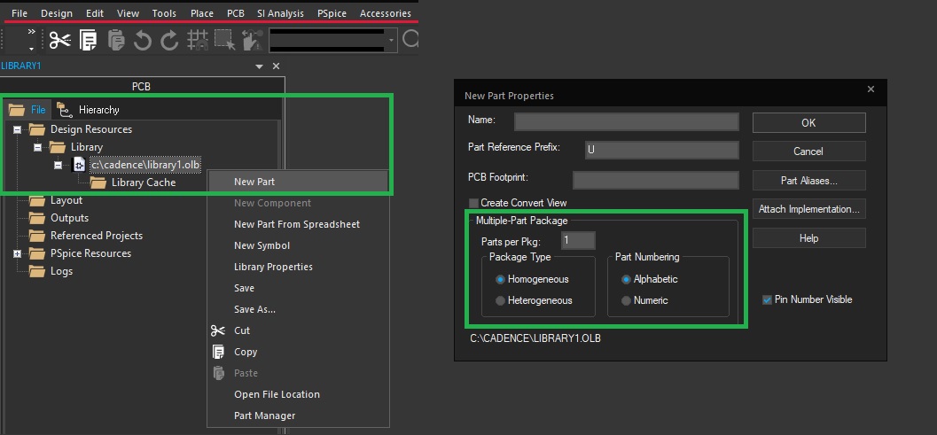
In the case where a separate library is desired, the user can open the schematic tool and select File -> New -> Library. The design navigation window will be updated to show the new .olb file which can be selected to Add a new part. Another window will be presented which requires the user to provide details pertaining to the component.
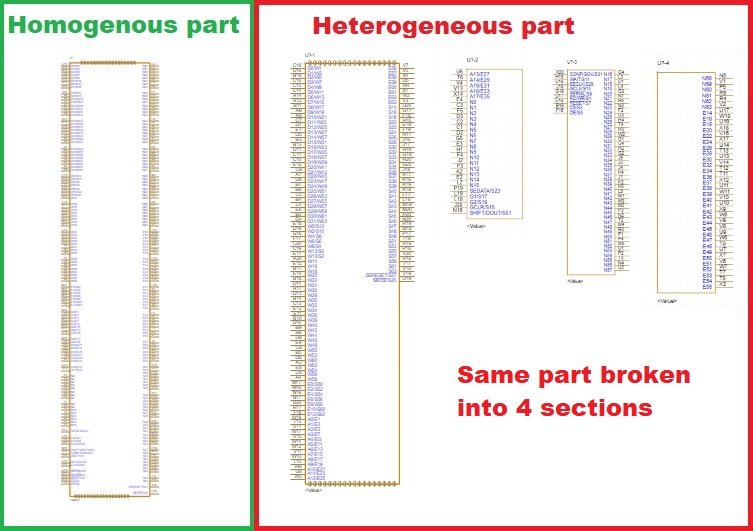
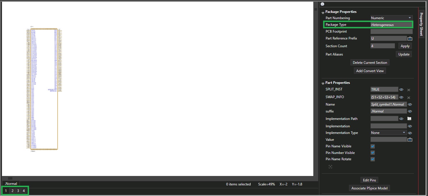
Simple parts found in a single package with a limited pin count are often classified as Homogeneous. For complex components, there are two reasons they need to be created as a Heterogeneous part. Either the package has multiple functional parts within it, such as dual transistors, or the pin count is high enough to warrant creating separate symbols so they can be used across several schematic sheets. Examples of the cases described above can be seen in the illustration.
Now that we understand the difference between a homogeneous part and heterogeneous part, it’s worth mentioning the Split Part capability within Orcad CIS. A homogenous part in the library can be selected and broken up into as many sections as desired. The pins will have to be assigned a specific section based on how many sections are created and the tool will automatically reconfigure the schematic symbol.
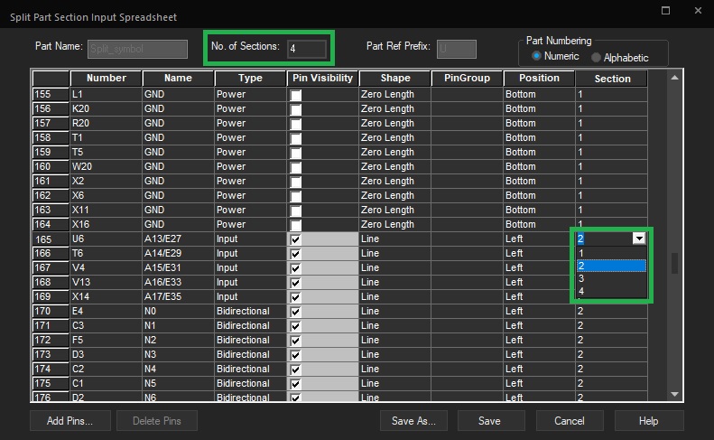
The additional tabs for each section will be created which allows the user to navigate between the sections and the Package type will be updated to Heterogeneous.
Defining properties and Pspice model
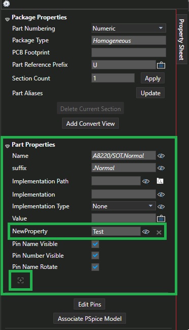
In the same Part Edit window, additional properties for the selected symbom will be visible which can be defined as desired. Depending on the component type, users often add relevant properties which allows a quick and easy method to filter when searching within existing parts. For example, if creating a symbol for a voltage regulator which may be added to an existing library, then common parameters such as Vin range and Vout may be useful properties to add.
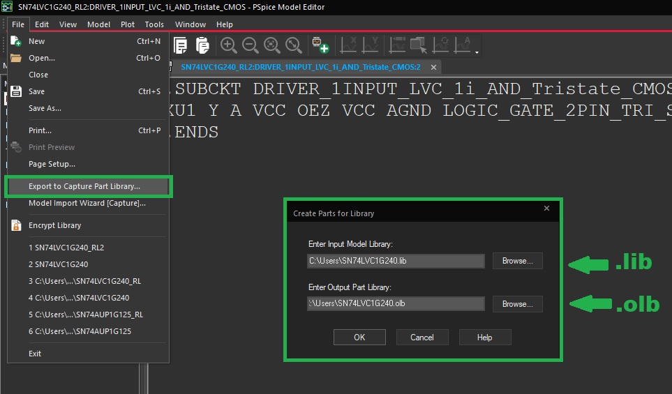
Another property which is relevant when simulations are intended is the PSpice model. This is often a .lib format file which is available from the component manufacturer. The PSpice model captures the behavioural characteristics of the component often defined over the working temperate range as well. This allows the designer to ensure the circuit behaves as intended across all desired operating conditions including corner cases. It’s probably worth mentioning that if a .lib file is available for the part of interest, then the designer can take advantage of another tool provided as part of the Cadence suite to quickly generate the respective schematic symbol. The PSpice model already captures the pin numbers, names, and type so it’s simply a matter of creating a visual representation in the form of a generic block schematic symbol. The PSpice Model Editor is a convenient tool which should be explored for the functionality as desired above. A single-click step (File -> Export to Capture Part Library…) allows the designer to save a .olb format file which can then be used in the schematic design. The PSpice model is automatically assigned as part of this process whereas, if the Model Editor is not used for creating the schematic symbol, then the PSpice Model will have to be associated as a separate step.
Adding to the design schematics and drawing connections
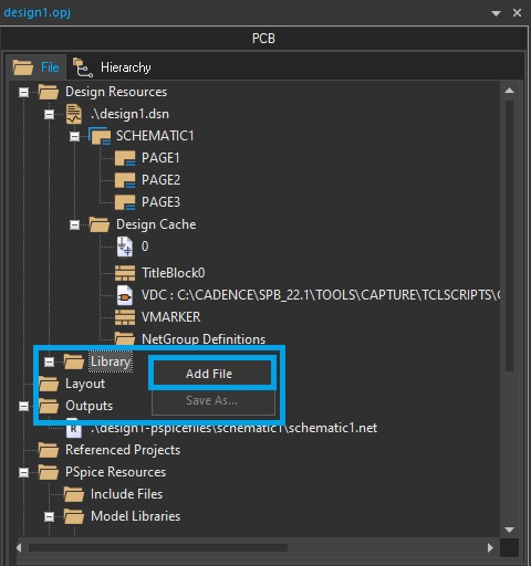
Once the schematic symbol part has been successfully created, then it's a straight-forward task to add it to the particular schematic design. Only key step involved here is to ensure the library is included in the design. Within the Design Resources structure, check the Library subfolder and confirm the respective library is being reference. If not, simply right-click on the Library subfolder and select "Add File". Navigate to the .olb file of interest and confirm it's accepted and available for use.
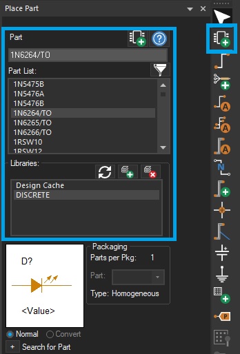
Now, to place the schematic symbol on a given schematic page, ensure the canvas is selected and visible before attempting any further steps. There are three methods to add a schematic symbol to the design. The shortcut key "P". Selecting Place->Part... from the Menu bar. Selecting the icon from the toolbar which looks like a 6-pin dual-in-line part with a + sign next to it. All methods will yield the same result which is to present the user with another window that lists all the schematics symbols within the newly added library. Upon selecting a particular part, the visual symbol will appear along with packaging information (homogeneous vs. heterogeneous). Double click the part of interest, hover over the area in the schematic canvas where you would like to place and part, and simply perform a left-click action. If no further schematic parts are desired, simply right-click anywhere on the schematic canvas and select "End Mode".
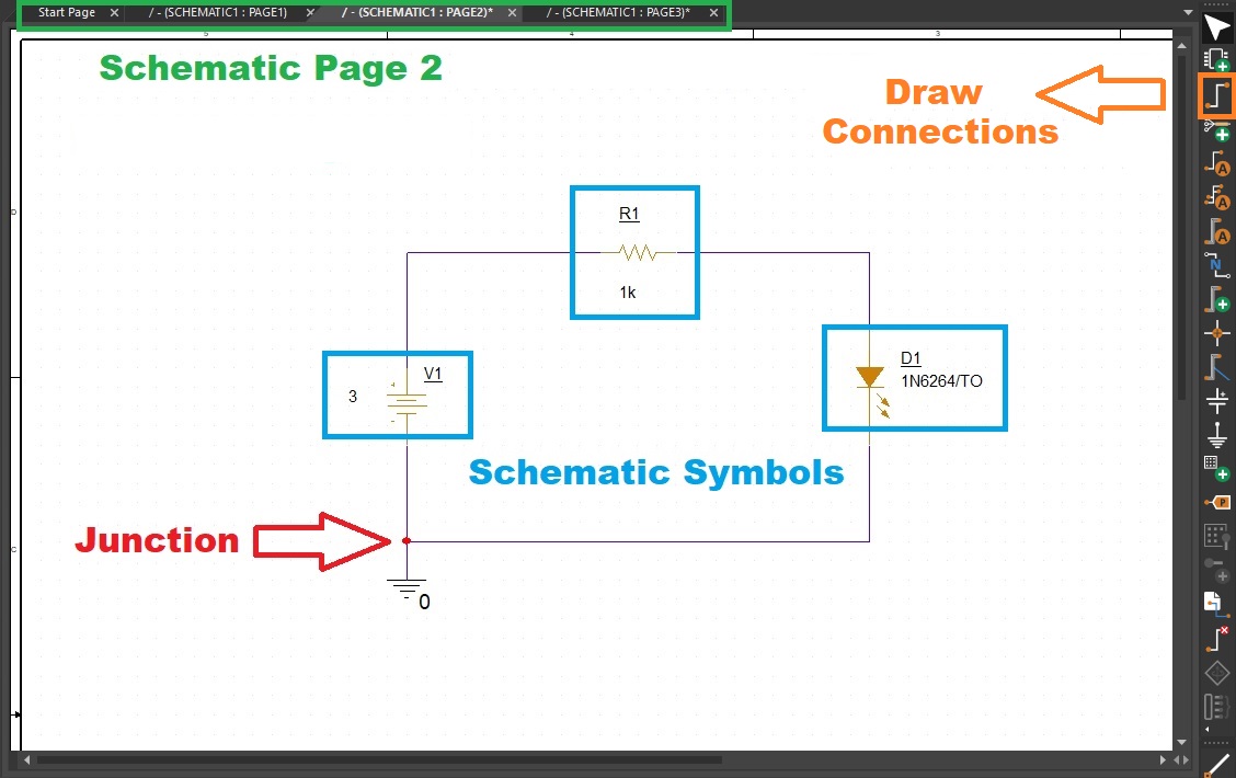
Drawing connections on the schematic canvas is another intuitive task which can be initiated by one of the following methods. Using the shortcut key "W", selecting Place->Wire from the menubar, or finding the icon in the toolbar which looks like 3-segment wire with dots on each end. Upon entering "Wire Mode", the arrow cursor will change to a cross-hair cursor. Single left-clicks will begin and end each segment of the wire. Junction connections (three connections or more at a point) will be visible by a coloured dot. Crossing wires will have no explicit indication so it is highly recommended to keep a clean and well-presented design to minimize such confusions. Assigning net names to each wire connection is also recommended which is a tremendous help for not only reabability but also a good design practise. The default assignment within the Cadence Schematic tool is a letter followed by a string of random integers. Almost all of the information captured during the schematic development phase will be propogated to the board layout hence it is critical shortcuts are not taken as this point. Be as clear and as explicit as possible. Assigning Reference Designators to the schematic symbols is another activity which should not be taken lightly as these will be identifiers for the respective parts until the end of life of the design.
Generate Netlist
In order to proceed to the layout phase of the project, the designer needs to generate the netlist. The netlist captures the logical connections between the components and translates the circuit information into a compatible format for layout design tools. In the case of the Cadence suite, the netlist can be created from Orcad Schematics Capture from the Tools Menu and clicking "Create Netlist...". The following dialog will be presented in which you can select the desired directory where you would like the netlist collateral to be generated.
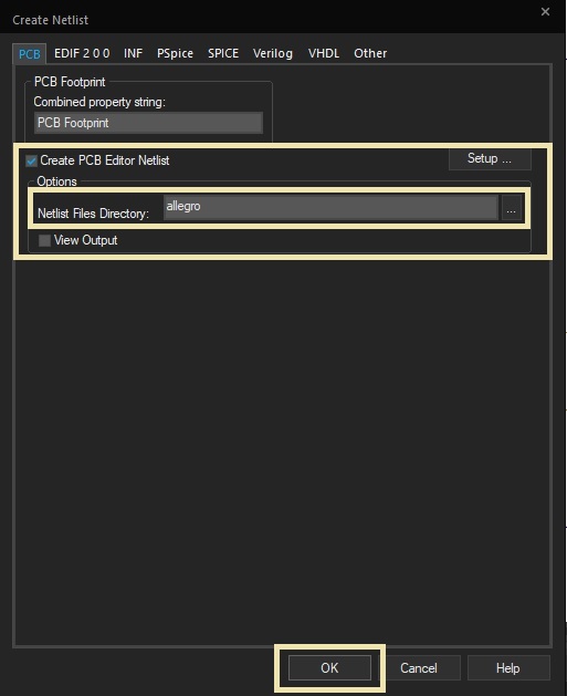
If no issues are highlighted with the wiring connections and component reference designators, then the following three files will be created in the selected directory: pstchip, pstxnet, and pstxprt. These are required in order to import the netlist into Cadence Allegro PCB Editor.
Component Placement
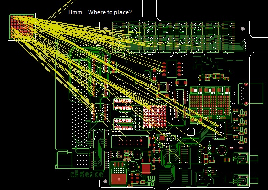
Careful placement of components is critical to a successful design
Capture CIS
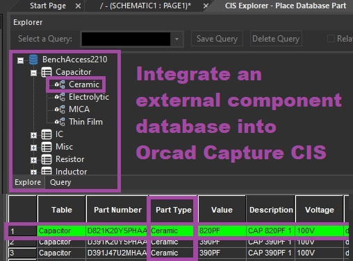
Set up an external component database and integrate with OrCAD Schematic Capture CIS
Generate Gerbers