Welcome to PCB PRO!
You'll find an abundance of resources to help you in your journey to become proficient in the art of designing Printed Circuit Boards. The content covered is primarily around usage of the Cadence Schematics and PCB Editor tools but also includes basic principles for circuit board design, high speed signal routing, and even insight on the manufacturing and assembly process. You'll find numerous links in the Menu sidebar which will help you navigate to sections of interest.
And of course, nothing is more interesting than light humour so dig into some PCB Jokes to spark up some inspiration!

This website is not structured as a course but rather an accummulation of posts providing in depth instructions on how to complete certain task using the Cadence EDA tools. Efforts are made to provide detailed illustrations in the posts but if that doesn't suffice, feel free to watch the focused YouTube videos which also take a step by step approach.
In addition, the content will feature less-known capabilities of the Cadence tool which will greatly enhance the user experience. It could be as simple as saving a customized colour template which can be reloaded when the tool is opened to provide a consistent working environment. Or a significant time saving feature such as the sub-drawing import/export which replicates the more traditional copy and paste functionality within the PCB Editor tool. Take your time in exploring these unique and hidden gems as you delve into the world of circuit board design and of course if you have any comments, questions, or concerns, don't hesitate to send a quick email thru the contact page.
CAD tools
A brief introduction to the CAD tools offered by Cadence to initiate schematic creation and board design
Design Overview
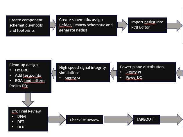
A high level overview of the design and development process depending on project complexity
PCB Stackup
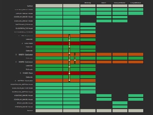
Setting up the PCB stackup in Allegro Cross-Section Editor
Component Placement
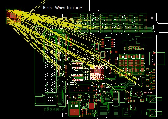
Careful placement of components is critical to a successful design
Sub-Drawing Feature
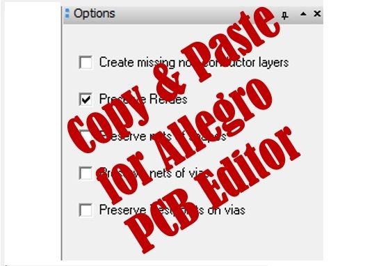
Convenient method to export sections of a design and export them into a new one.
Generate Gerbers
PCB fabrication is dependent upon the final Gerber dataset as delivered by the designer
Routing Traces
Diligent routing is critical to ensure a successful design
Shapes
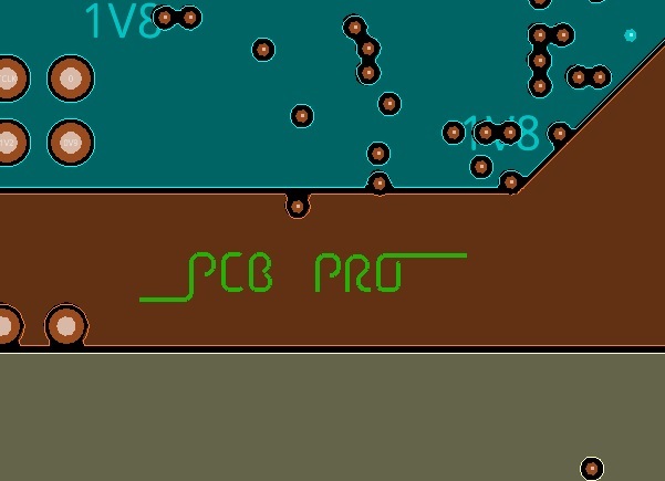
Pour large regions of copper in your design using shapes
Constraint Manager
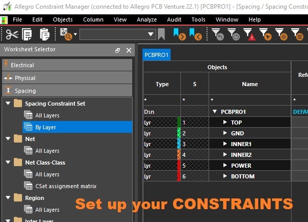
Defining constraints accurately and early in the design cannot be stressed enough!
Z-Copy
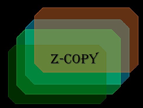
Best kept secret in Allegro PCB Editor for copying shapes across layers
Thermal Relief
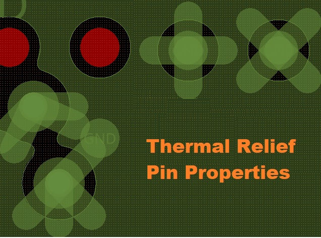
Pour large regions of copper in your design using shapes
Color Settings
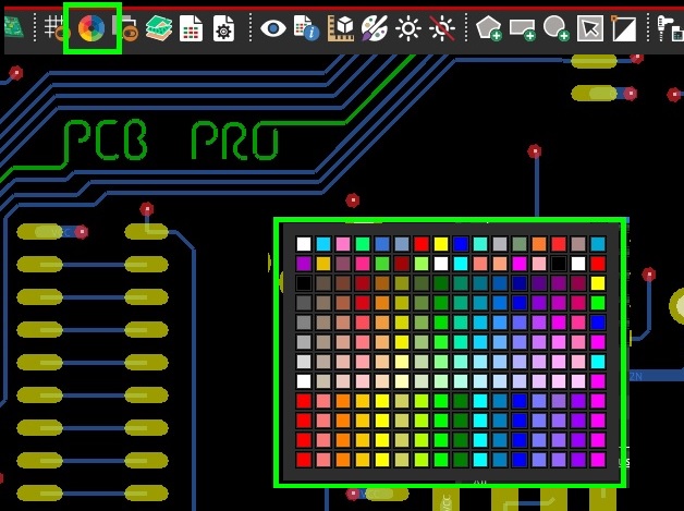
Customize Allegro PCB Editor color settings to enhance usability
Schematic Capture
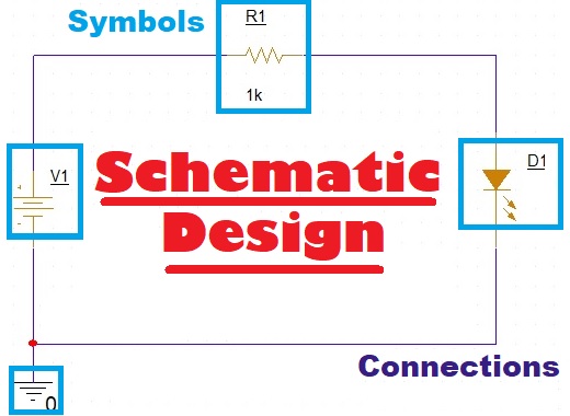
Creating schematic symbols, drawing the circuit, and generating the netlist
Capture CIS
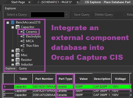
Set up an external component database and integrate with OrCAD Schematic Capture CIS
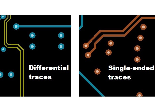
Trace Length Matching
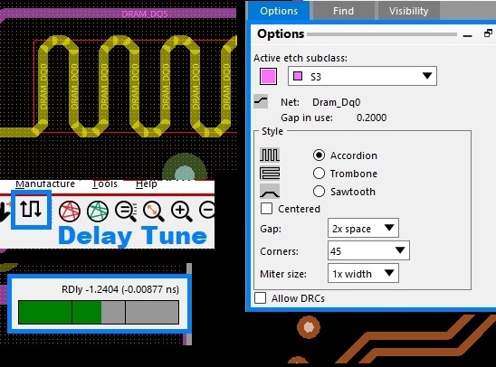
High speed interface signal traces need to be length matched to ensure correct operation
Silkscreen Markings
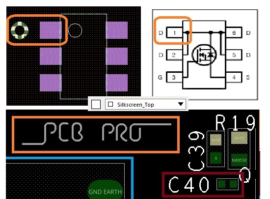
Learn how to add key silkscreen markings to your design in Allegro PCB Editor
High Speed Design

Learn fundamentals of High Speed PCB Design
Add 3D STEP Models

Learn how to add 3D STEP models to symbol footprints
Text Blocks


