Intro to Cadence Schematic and PCB Design Tools
Article published Nov 6th 2022!
As you begin your journey in the world of Hardware Design, you'll come across several CAD software tools. A prominent one in the industry is the Cadence suite which is utilized both among students and professionals. Cadence has done an excellent job not only updating it's offering in terms of features and capabilities as per industry advancements, but also modernizing the Graphical User Interface. Over time, tool usage has become much more intuitive and accepted by the community.
Intro to Schematics Capture
Schematics capture is intended for the designer to create the logical connections between the components used in their electrical project. The schematics can either be a flat design which means off-sheet connectors are used to link the nets or it can be a hierarchical design which involves having modular blocks that can be reused. Often enough, simpler designs are created using a flat method whereas complex designs deploy the hierarchical approach. Regardless of which style is utilized, the steps involved in creating the schematic components, drawing wires to make the logical connection, and assigning reference designators are required. This will then allow the designer to generate the netlist which is imported into the accompanying layout tool known as Allegro PCB Editor.

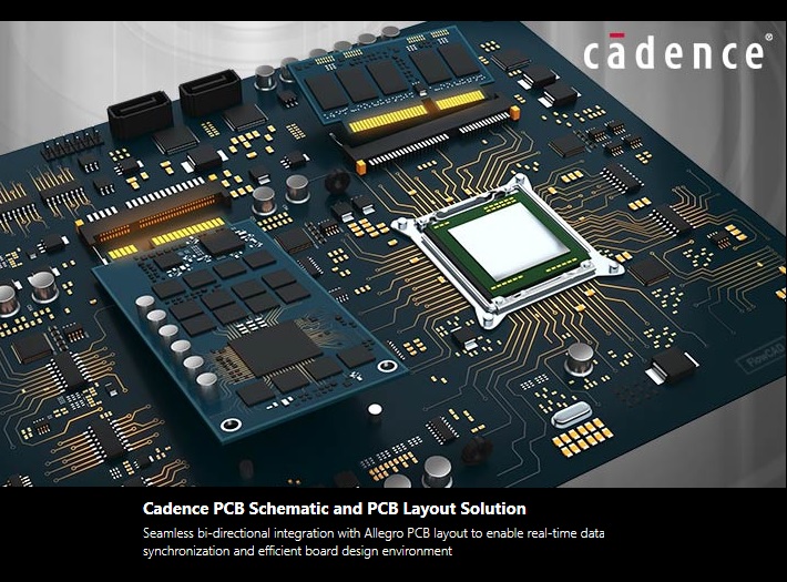
Intro to Allegro PCB Editor
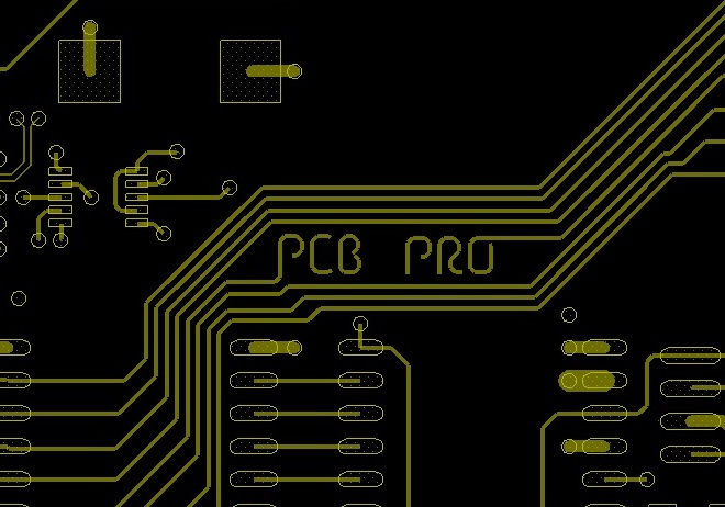
The physical placement of the components in a given design are captured in the layout tool. Upon importing the netlist which was created from the schematics capture tool, the designer assigns locations of each part and draws the wiring. Depending on the complexity of the design, a single layer Printed Circuit Board (PCB) may be used or a multi-layer board. Allegro PCB Editor is used to capture the PCB stackup and dimensions and the complete design routing. These details are then exported in a gerber dataset or similar format and sent to the PCB fabrication house where the manufacturing happens.

Other tools
Depending on the complexity of the design, other EDA tools may also be required. For projects which feature a high speed electrical interface, simulations are often recommended to ensure the timing and signal integrity meet design specifications. There are dedicated tools offered by various vendors including Sigrity Suite by Cadence. Sigrity SI is targeted for high speed signal integrity interface simulations such as NAND, DRAM, and SPI whereas Sigrity PI is focused around Power Delivery Network simulations. Both types of analysis are critical for a successful design.

Summary
In conclusion, hardware design is at a minimum two step process which includes creating the schematics and then completing the circuit board layout and routing. The Cadence suite is a great toolset for accomplishing these tasks and this blog will hopefully illustrate some cool features, tips, and tricks to make your journey on this adventure that much more enjoyable!
Watch Demo! - Like & Subscribe!
Component Placement
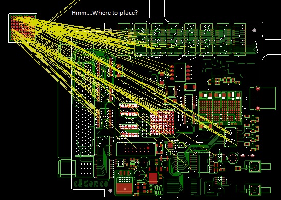
Careful placement of components is critical to a successful design
Sub-Drawing Feature
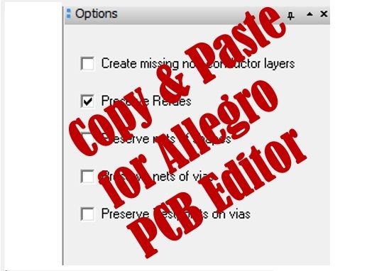
Convenient method to export sections of a design and export them into a new one.
Generate Gerbers