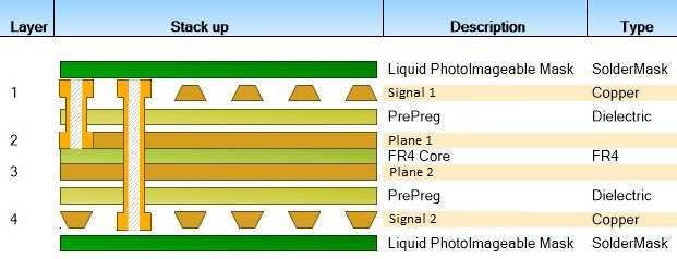
Defining the PCB Stackup
Article published Nov 12th 2022!
A critical step as the design is initiated is to ensure the appropriate PCB stackup is defined. This often involves a discussion with the circuit board manufacturer to confirm the following details at a minimum:
Depending on the complexity of the design, additional parameters may also need to be defined. In the case of a PCB with high speed electrical interfaces, low-loss materials may be necessary to minimize insertion and return loss. This will impact the signal integrity therefore affecting the speed at which the interface will operate. If the design is extremely dense and board real estate is a premium, then embedded components may be a suitable option. This will require adopting a unique stackup to ensure the appropriate layers are defined for where cavities may exist. Those are two examples where additional details needs to be defined when deciding upon a stackup. For the majority, the basic parameters around layer count and copper features are often sufficient and can be captured in the EDA tool.
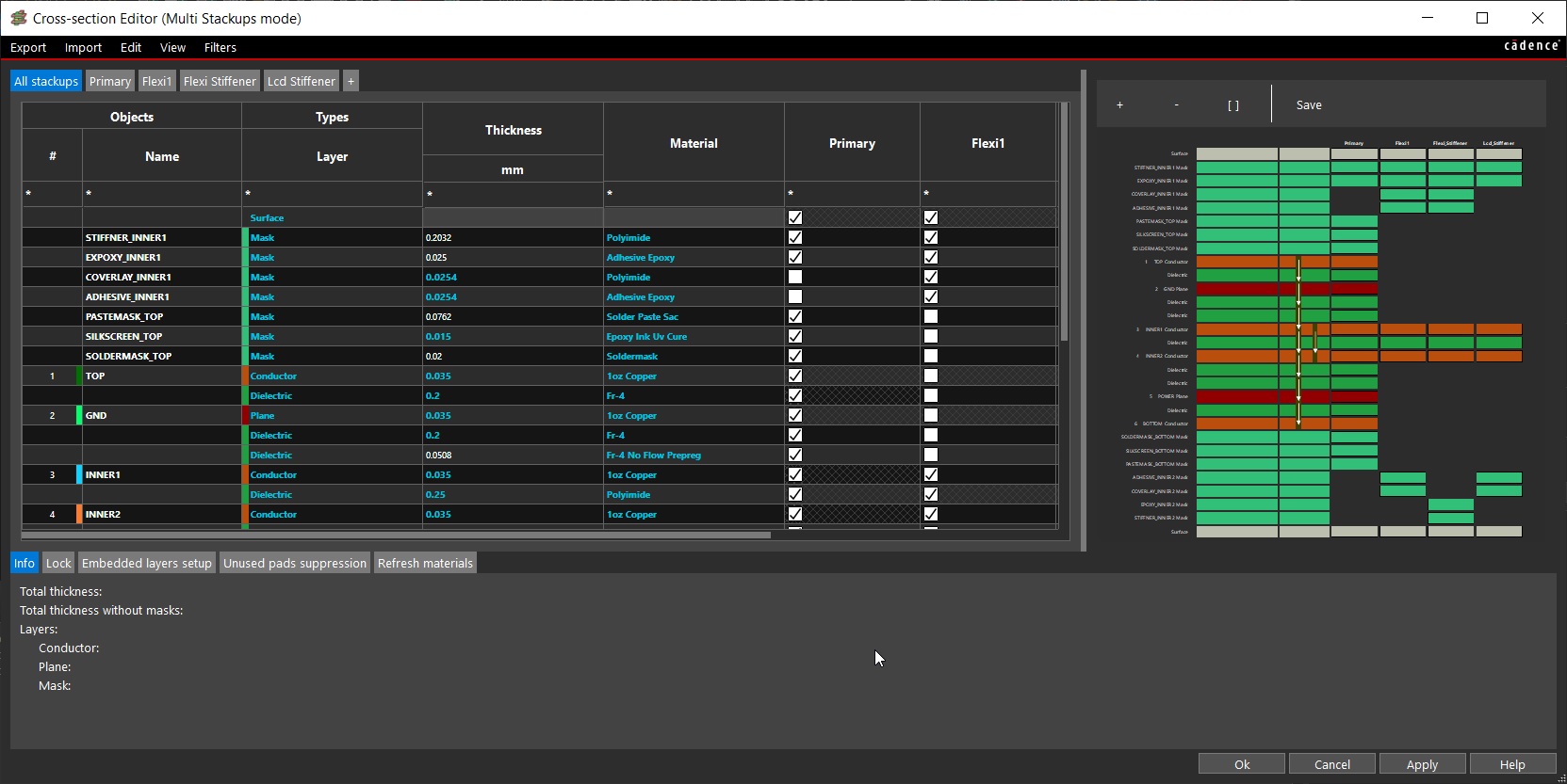
Input Stackup Details
Allegro PCB has an intuitive cross-section editor which captures the stackup details. There are multiple methods to import the stackup details with the easist one being an IPC2581 format file. This is an XML file which PCB fab houses are able to provide that the Cadence Allegro tool accepts. Another format which is commonly used is the Technology file (.tcf). This is often useful when exchanging stackup details within EDA tools. Lastly, there is the manual method which requires individual update to each cell based on details provided by the PCB vendor. This is both a labour intensive and tedious task which is prone to human error but also potentially useful when only a minor modification is required. Regardless of which method is used to update the stackup details, the Allegro Cross-Section Editor is a sophisticated tool essential in capturing one of the most critical steps in designing a Printed Circuit Board.
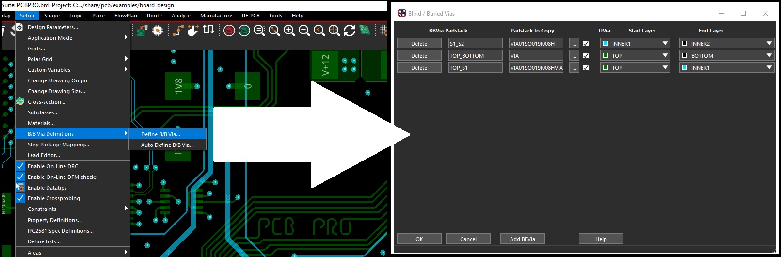
Define Via Structure
Routing traces often requires traversing thru different layers and therefore plated holes connecting these layers, known as vias, are required throughout the design. Depending on the complexity of the design, a combination of thru-hole, blind, and buried vias are necessary. The higher the layer count, the more complex the via structure. These details are often communicated in the stackup discussion with the PCB vendor and once finalized, they need to be captured in the EDA tool. For the case of Allegro PCB Editor, the via structure is defined under Setup -> B/B Via Definition -> Define B/B Via...
The following window will be presented which can be used to specify the Start and End layers for the desired via. An appropriate name is recommended so that when one is routing the traces and needs to jump between layers, they can easily select the via as needed.
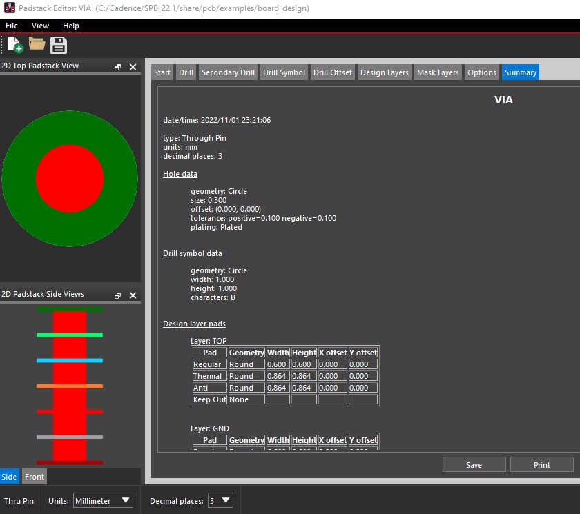
In order to define the via itself and it's respective properties, the padstack editor is deployed. The designer has numerous options to select from including the drill hole size, anit-pad clearance, pad size, and film definitions. This via definition is saved as a .pad format file and the location is mapped to the padpath variable so Allegro knows where to look for this particular pad.
Summary
Defining the stackup along with the via structure is a critical task the designer must complete before any form of placement and routing can be initiated. This information is key to the success of a design both in terms of schedule and cost. Not having a well defined stackup as per the complexity of the design will result in headaches when it comes time to do the component placement and routing. Changes late in the design cycle will have a ripple effect so it's highly recommended proper consideration be given to this particular task. When in doubt, opt for a higher layer count than necessary as it's less effort to remove extra routing layers compared to adding layers and using them appropriately.
Watch Demo! - Like & Subscribe!
Component Placement
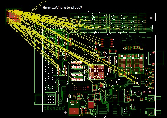
Careful placement of components is critical to a successful design
Silkscreen Markings
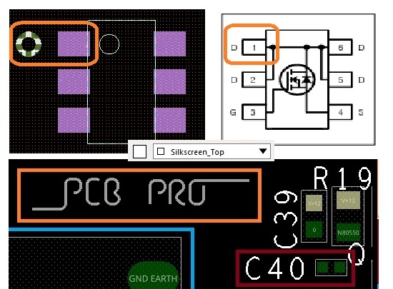
Learn how to add key silkscreen markings to your design in Allegro PCB Editor.
Generate Gerbers