Fundamentals of High-Speed Design
Article published April 2nd 2024!
In today's technologically advanced world, high-speed Printed Circuit Board (PCB) design is at the forefront of innovation, driving the development of a wide range of electronic devices, from smartphones and computers to sophisticated medical instruments and aerospace systems. As the demand for faster and more efficient electronic products continues to grow, so does the importance of mastering the fundamentals of high-speed PCB design.

Designing a high-speed PCB requires a meticulous approach that encompasses various factors, including signal integrity, power distribution, electromagnetic interference (EMI), and thermal management. Let's delve deeper into each of these key aspects:
Layer Stackup
The layer stackup is the foundation of any PCB design, and it becomes particularly critical in high-speed designs. A well-planned layer stackup involves strategically arranging multiple signal layers, ground planes, and power planes to minimize signal interference and impedance mismatches. High-speed designs often utilize controlled impedance routing to maintain signal integrity, ensuring that signals propagate efficiently without distortion.
Signal Integrity
Signal integrity is paramount in high-speed designs to ensure the reliable transmission of data without distortion or degradation. Factors such as trace length, impedance matching, and signal termination play crucial roles in preserving signal integrity. Controlled impedance routing techniques, differential signaling, and signal length matching are employed to mitigate signal reflections, crosstalk, and other sources of signal degradation.
Routing Techniques
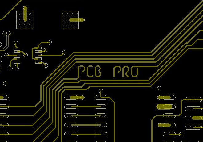
Efficient routing is essential for high-speed PCBs to minimize signal degradation and EMI. Differential pairs, high-speed signals, and clock lines require careful routing techniques to maintain signal integrity. Techniques such as length matching, avoiding right-angle bends, and reducing the number of vias help optimize signal transmission and minimize signal distortion.
Power Distribution
Proper power distribution is vital for stable operation and preventing voltage drops, especially in high-speed designs with numerous components drawing varying currents. Decoupling capacitors, power planes, and careful component placement are utilized to minimize power distribution network impedance and ensure adequate power delivery to all components.
Electromagnetic Compatibility (EMC)
High-speed PCBs are susceptible to electromagnetic interference (EMI), which can adversely affect nearby components and disrupt the functionality of the device. Shielding, grounding, and careful layout design are employed to mitigate EMI issues and ensure compliance with EMC standards. Techniques such as signal isolation, ground plane partitioning, and ferrite beads are used to suppress EMI and maintain signal integrity.
Thermal Management
High-speed designs often generate significant heat due to the high-frequency operation of components. Effective thermal management is crucial to prevent overheating and ensure the reliability of the PCB. Techniques such as thermal vias, heat sinks, and proper component placement help dissipate heat and maintain optimal operating temperatures, ensuring the longevity and reliability of the electronic device.
Design Validation and Simulation
Before fabrication, high-speed PCB designs undergo rigorous validation and simulation to identify and address potential issues. Advanced simulation tools, such as signal integrity simulators, electromagnetic field solvers, and thermal analysis software, are employed to analyze the performance of the design and optimize its parameters. By simulating signal integrity, thermal behavior, and EMI susceptibility, engineers can fine-tune their designs and ensure their reliability and performance in real-world applications.

Summary
In conclusion, mastering the fundamentals of high-speed PCB design is essential for engineers striving to develop reliable and high-performance electronic devices. By understanding and implementing techniques such as proper layer stackup, signal integrity optimization, efficient routing, and robust EMC mitigation, engineers can ensure the success of their high-speed PCB designs in today's demanding technological landscape.
Component Placement
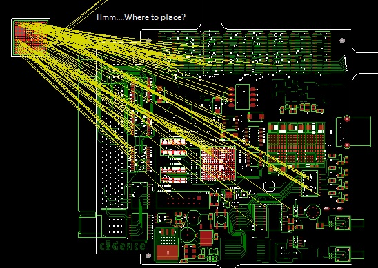
Careful placement of components is critical to a successful design
Schematic Capture
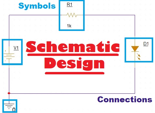
Creating schematic symbols, drawing the circuit, and generating the netlist
Generate Gerbers